


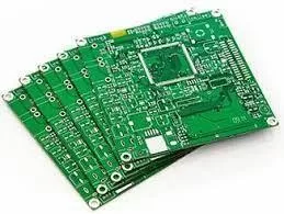
What’s PCBA?
 1280
1280Global electronic component supplier AMPHEO PTY LTD: Rich inventory for one-stop shopping. Inquire easily, and receive fast, customized solutions and quotes.
What is PCBA?
PCBA stands for Printed Circuit Board Assembly. The act of constructing an operational electronic device by placing electronic components onto a printed circuit board (PCB) is known as PCB assembly. PCBA is an essential step in the manufacturing of various electronic products, including computers, smartphones, home appliances, and industrial equipment. During the PCBA process, electronic components such as resistors, capacitors, integrated circuits, connectors, and other active and passive devices are soldered onto the PCB. These components are carefully placed and soldered onto the designated areas of the PCB according to the circuit design.
The process of PCBA generally includes the subsequent stages:
Component Procurement: The first step is to source and procure the required electronic components for the PCB assembly. This includes identifying the specific components needed and ensuring their availability and quality.
PCB Fabrication: The PCB is fabricated by printing the circuit design onto a board made of insulating material, such as fiberglass-reinforced epoxy. This involves the process of etching, which removes excess copper to create the desired circuit pattern.
Component Placement: Once the PCB is ready, the electronic components are placed onto the board according to the circuit design. This can be done manually or using automated machines, depending on the scale of production. Automated component placement machines are often used for high-volume production to ensure accuracy and efficiency.
Soldering: After the components are placed on the PCB, soldering is performed to establish electrical connections. Solder, a low-melting-point alloy, is melted and applied to the component leads and the copper pads on the PCB. This creates a strong and reliable bond between the components and the PCB.
Inspection and Testing: Once the soldering is complete, the assembled PCBs undergo inspection and testing to ensure quality and functionality. This involves visual inspection to check for any soldering defects or component placement issues. Functional testing may also be performed to verify that the assembled electronic device operates correctly.
Packaging and Shipping: The final step involves packaging the assembled PCBs into suitable enclosures or protective packaging. This can include placing the PCBs into cases, adding labels or documentation, and preparing them for shipment to customers or further manufacturing processes. PCBA requires expertise, precision, and adherence to quality standards to ensure the reliable operation of electronic devices. It is a critical process in the electronics manufacturing industry, enabling the production of various electronic products that we use in our daily lives.
Types of PCBA Process
PCBA processes vary based on factors like component types, board complexity, size, performance requirements, cost considerations, and manufacturing capabilities. Different types and combinations of methods can be used to meet specific needs, so here I list several processes that are most commonly seen in daily life.
Through-Hole Technology (THT)
In THT assembly, electronic components with leads (pins) are inserted into pre-drilled holes on the PCB. The leads are then soldered on the opposite side of the board to establish electrical connections. THT is suitable for more significant components, high-power applications, and when mechanical strength is required. THT offers benefits such as mechanical strength, ease of repair and rework, and suitability for high-power applications. However, it has limitations in terms of component size, density, and the additional space required for the leads and holes on the PCB.
Surface Mount Technology (SMT)
SMT is the most widely used PCBA method. It involves mounting components directly onto the surface of the PCB, without the need for drilling holes. The components have solder pads on their undersides, which are soldered onto the corresponding pads on the PCB. SMT allows for smaller component sizes, higher component density, and automated assembly processes.
For more information, please read this blog: Surface Mount Technology (SMT) Basic and Its Process.
Mixed Technology
Mixed technology PCBAs combine both through-hole and surface-mount components on the same board. Some components may be mounted using THT, while others are mounted using SMT. This approach is used when certain components are not available in surface mount packages or when specific requirements call for THT components.
Ball Grid Array (BGA) Assembly
BGAs are a type of surface mount package in which solder balls are located on the underside of the component. BGAs offer high pin densities and excellent electrical performance. BGA assembly involves precise alignment and soldering of the solder balls to corresponding pads on the PCB. Advanced techniques such as reflow soldering or ball grid array rework are used for BGA assembly.
Chip-on-Board (COB) Assembly
In COB assembly, bare semiconductor chips are directly mounted onto the PCB substrate without a traditional package. The chip is wire-bonded and then encapsulated with an epoxy or other protective material. COB is commonly used for applications where size and weight reduction are critical, such as in mobile devices and wearables.
Flexible PCB Assembly
Flexible Printed Circuit Boards (Flex PCBs) are made from flexible substrate materials, allowing them to bend and conform to different shapes. Flexible PCB assembly involves mounting components onto these flexible substrates using SMT or other suitable methods. Flex PCBs are used in applications that require flexibility, such as curved displays, wearable devices, and automotive electronics.
PCB VS PCBA
Here's a chart comparing PCB (Printed Circuit Board) and PCBA (Printed Circuit Board Assembly):
| Aspect | PCB | PCBA |
| Definition | Physical board providing electrical connections | PCB with electronic components assembled |
| Components | Does not include electronic components | Includes electronic components |
| Manufacturing | Involves processes like etching, drilling, solder mask application | Component placement, soldering, inspection, testing |
| Functionality | Provides mechanical support and electrical connections | Creates fully functional electronic devices |
| Expertise | Requires knowledge of PCB design and manufacturing | Requires expertise in component placement and soldering |
| Design | Designed using software tools and techniques | PCB design includes component footprints and soldering pads |
| Testing | PCB functionality is not tested as part of the PCB manufacturing process | Assembled PCBA undergoes functional testing |
| Applications | Used as a base for assembling electronic circuits | Used in various electronic devices and systems |
| Complexity | Can vary from simple single-layer boards to complex multi-layer boards | Complexity increases with the number of components and layers |
| Production | Can be manufactured in-house or outsourced | Often outsourced to specialized electronics manufacturers |
| Cost | Cost depends on board size, complexity, and manufacturing processes | Cost depends on component costs, assembly complexity, and testing requirements |
For more information about PCB, please click here.
PCBA Design
The process of arranging electronic components on a printed circuit board (PCB) for assembly is known as PCBA design. This involves transforming the circuit schematic into a physical design that can be produced and assembled.
Usually, the process of designing PCBA involves the following stages:
Circuit Schematic Design: The first step is to create the circuit schematic, which represents the electrical connections and components of the electronic device. This is typically done using electronic design automation (EDA) software, such as Altium Designer or Eagle.
Component Selection: Once the circuit schematic is complete, the next step is to select the appropriate electronic components for the design. This includes considering factors such as component specifications, availability, cost, and compatibility with the design requirements.
PCB Layout Design: In this step, the PCB layout is created, which involves placing the electronic components on the PCB and routing the electrical connections between them. The layout must consider factors such as component placement, signal integrity, power distribution, and thermal management.
- Component Placement: The electronic components are placed on the PCB according to their physical and electrical requirements. Placement considerations include minimizing signal interference, optimizing signal flow, and ensuring proper clearance between components.
- Routing: Once the components are placed, the electrical connections, or traces, are routed between them. This involves determining the optimal path for each connection while considering factors such as signal integrity, impedance control, and noise reduction. The routing process can be done manually or using automated routing tools.
Design Rule Check (DRC): After the PCB layout is complete, a Design Rule Check is performed to ensure that the design meets the manufacturing and assembly requirements. This involves verifying that the layout follows design rules related to trace width, spacing, clearance, and other manufacturing constraints.
Gerber File Generation: Once the PCB layout passes the DRC, the design files, including Gerber files, are generated. Gerber files contain the necessary information for PCB fabrication, including the copper layers, solder mask, and component placement. PCBA design requires expertise in electronics, an understanding of PCB manufacturing processes, and knowledge of design guidelines and standards. It is crucial to consider factors such as component placement, signal integrity, thermal management, and manufacturability to ensure the functionality and reliability of the final electronic device.
PCBA design software is commonly used to facilitate the design process and generate the required files for PCB fabrication and assembly. Additionally, collaboration with PCB manufacturers and assembly houses can be beneficial to ensure a successful PCBA design and production process.
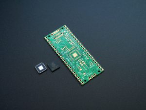
PCBA Board
A PCBA board, also known as a Printed Circuit Board Assembly board, refers to the combination of a printed circuit board (PCB) and the electronic components that are mounted on it. It is a crucial component of electronic devices and serves as the foundation for the electrical connections and functionality of the device. The PCBA board consists of two main elements:
Printed Circuit Board (PCB): The PCB is a flat board made of non-conductive material, typically fiberglass-reinforced epoxy, with a thin layer of copper foil on one or both sides. It provides a platform for mounting and interconnecting electronic components. The PCB design includes copper traces, vias, and pads that form the electrical pathways between components.
Electronic Components: The electronic components are the active and passive devices that are mounted on the PCB. These components include integrated circuits (ICs), resistors, capacitors, inductors, diodes, transistors, connectors, and more. Each component has its function and plays a specific role in the overall operation of the electronic device. The PCBA board manufacturing process involves several steps:
PCB Fabrication: The PCB fabrication process starts with the production of the bare PCB. It involves the etching of copper layers, drilling holes, and applying a solder mask and silkscreen to indicate component placement and labeling.
Component Placement: Once the bare PCB is ready, the electronic components are placed on the board according to the PCBA design. This can be done manually for low-volume production or using automated pick-and-place machines for high-volume production.
Soldering: After component placement, the next step is soldering, which involves permanently attaching the components to the PCB. There are two commonly used methods for soldering: through-hole soldering and surface-mount technology (SMT) soldering. Through-hole soldering involves inserting component leads through holes in the PCB and soldering them on the other side. SMT soldering, on the other hand, involves attaching components directly to the surface of the PCB using solder paste and a reflow oven.
Inspection and Testing: Once the soldering process is complete, the PCBA board undergoes inspection and testing. This includes visual inspection to ensure proper component alignment and solder joints, as well as electrical testing to verify the functionality and performance of the assembled board.
Final Assembly: After passing inspection and testing, the PCBA boards are ready for final assembly into the complete electronic device. This may involve additional steps such as enclosure assembly, wiring, and final testing before the product is prepared for shipment.
Conclusion
To summarize, we explored PCBA (Printed Circuit Board Assembly), which is the process of assembling electronic components onto a PCB to create functional electronic devices. We also discussed the steps involved, from procurement to testing. Different PCBA methods include THT, SMT, BGA assembly, and COB assembly. Each method has its advantages and is chosen based on the specific requirements of the electronic device being manufactured. Whether you are an electronics enthusiast or a professional in the industry, this blog has provided you with a solid foundation to grasp the basics of PCBA. It is an essential aspect of electronics manufacturing, shaping the devices we rely on daily. Now armed with this knowledge, you can delve further into the world of PCBA, explore advanced techniques, and appreciate the intricate craftsmanship behind the electronic devices we use and rely on every day.