


What Is PCB, and How Does It Work?
August 15 2023  1470
1470
1470Inquiry
Global electronic component supplier AMPHEO PTY LTD: Rich inventory for one-stop shopping. Inquire easily, and receive fast, customized solutions and quotes.
QUICK RFQ
ADD TO RFQ LIST
In this blog, we delve into the world of PCB (Printed Circuit Boards) and explore its fundamental role in electronic devices. Discover what PCB is, and how it works. Gain a clear understanding of the inner workings of PCBs and their significance in modern technology.
What PCB Stands for?
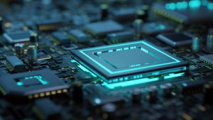
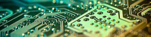
PCB stands for "Printed Circuit Board." It is a flat board made of non-conductive material, such as fiberglass or composite epoxy, with conductive pathways etched or printed onto its surface. These pathways, also known as traces, are used to connect and provide electrical connections between electronic components mounted on the board. PCBs are widely used in electronic devices and are a fundamental part of modern electronics manufacturing.What is PCB?
A printed circuit board (PCB) is a fundamental component of modern electronic devices. It serves as a platform for interconnecting and supporting electronic components, enabling the smooth flow of electrical signals. PCBs consist of a non-conductive board, typically made of fiberglass, with thin copper traces etched or printed onto its surface. These copper traces form the pathways for electrical current to travel between components. PCBs can have single-layer, double-layer, or multi-layer designs, depending on the complexity of the circuit. The components, such as resistors, capacitors, integrated circuits, and connectors, are soldered onto the PCB, forming a complete electronic assembly. PCBs offer numerous advantages, including compactness, reliability, and ease of mass production. They simplify the assembly process, reduce wiring errors, and enable efficient production of electronic devices. From consumer electronics like smartphones and computers to industrial equipment and medical devices, PCBs play a vital role in powering our modern technological world. In the electronics sector, PCBs are frequently utilized to offer a portable and dependable substrate for constructing and connecting electrical circuits.Types of PCBs
There are several types of PCBs available, each designed to meet specific requirements and applications. Single-Sided PCB: This is the simplest type of PCB, with components mounted on one side and copper traces on the other. They are cost-effective and commonly used in simple electronics. Double-Sided PCB: These PCBs have copper traces on both sides, allowing for more complex circuitry and increased component density. Components are mounted on both sides, and vias are used to provide interconnections between the layers. Multilayer PCB: Multilayer PCBs consist of multiple layers of copper traces separated by insulating material. They offer higher component density and better signal integrity. The layers are interconnected using vias, and they are commonly used in advanced electronics like computers, smartphones, and high-speed communication devices. Rigid PCB: Rigid PCBs are made of solid, inflexible materials like fiberglass or epoxy. They provide robustness and stability, making them suitable for applications where the board needs to maintain its shape and withstand mechanical stress. Flexible PCB (Flex PCB): These PCBs are made of flexible materials like polyimide, allowing them to bend and conform to different shapes. Flex PCBs are used in applications where space constraints, vibration, or movement require a flexible board. Rigid-Flex PCB: Rigid-flex PCBs combine rigid and flexible PCBs, providing a combination of stability and flexibility. They are suitable for devices that require both rigid and flexible sections, allowing for complex designs and compact form factors. High-Frequency PCB: These PCBs are designed to handle high-frequency signals without significant signal loss or interference. They feature specialized materials and precise trace layouts to maintain signal integrity and control impedance. High-Density Interconnect (HDI) PCB: HDI PCBs are designed to maximize component density and reduce the overall size of the board. They employ advanced manufacturing techniques, such as micro vias and fine-pitch components, to achieve higher circuit density.How PCB is Made?
The manufacturing process of a printed circuit board (PCB) involves several steps. Design and Prototyping Schematic Design: The circuit design is created using Electronic Design Automation (EDA) software, representing the connections between components. PCB Layout Design: Components are placed and interconnected on the board using the EDA software. Design rules are defined, including trace widths, clearances, and pad sizes. Prototyping: A prototype PCB is typically manufactured to validate the design and identify any issues before mass production. PCB Fabrication Substrate Preparation: A layer of non-conductive material, typically fiberglass-reinforced epoxy resin, is coated with a copper foil on one or both sides. Photoresist Application: A layer of photoresist material is applied to the copper surface, which is then exposed to UV light through a photomask containing the desired circuit pattern. Etching: The unexposed photoresist is removed, leaving behind the protected copper traces. The board is then etched in an acidic solution to remove the excess copper, leaving the desired circuitry. Plating: Copper is plated onto the remaining exposed copper surfaces to increase their thickness and ensure proper conductivity. Solder Mask and Legend Printing: A solder mask layer is applied to protect the copper traces, and a legend layer is printed to indicate component placement and other information. Surface Finish: A surface finish coating, such as tin/lead (HASL), gold, silver, or immersion tin, is applied to protect the exposed copper and facilitate component soldering. Component Assembly Stenciling: A solder paste stencil is aligned and applied to the board to deposit solder paste onto the pads. Component Placement: Automated machines or manual labor place the components onto the board, aligning them with the corresponding pads. Soldering: The board is passed through a reflow oven, where heat melts the solder paste, creating a permanent connection between the components and the PCB. Inspection: Visual inspection and automated testing methods are employed to verify the quality of the solder joints and component placement. Testing and Quality Assurance Electrical Testing: The assembled PCBs undergo functional and electrical tests to ensure proper circuit operation. Quality Control: Visual inspection, automated optical inspection (AOI), and other quality control measures are conducted to identify any defects or issues.How PCB Works?
A PCB (Printed Circuit Board) works by providing a platform for electronic components to be mounted and interconnected through conductive traces, allowing the flow of electrical signals and power between the components. Here's a step-by-step explanation of how a PCB works: Design: The process begins with the design of the PCB layout using specialized software. The circuit designer determines the placement of components, the routing of traces, and the arrangement of layers based on the desired functionality and constraints. Fabrication: Once the PCB design is finalized, the fabrication process begins. It typically involves the following steps:- Substrate Preparation: The non-conductive substrate material, such as fiberglass or composite epoxy, is prepared in the desired shape and size for the PCB.
- Copper Cladding: Thin copper foils are laminated onto the substrate, typically on both sides, forming a conductive layer.
- Etching or Printing: The conductive copper layer is selectively removed using etching or printing techniques, leaving behind the desired pattern of conductive traces and pads that form the circuitry.
- Drilling: Holes are drilled into the PCB at specific locations to accommodate component leads and vias, which are used for electrical connections between different layers.
- Solder Mask and Silkscreen: A solder mask layer is applied to protect the copper traces and pads, leaving exposed areas for soldering components. A silkscreen layer is added for labeling and component identification.
- Surface Finish: A surface finish, such as a layer of solder or a metal coating, is applied to protect the exposed copper and ensure good solderability.
- Through-Hole Technology (THT): Components with leads are inserted into pre-drilled holes on the PCB, and the leads are soldered on the opposite side. This provides mechanical stability and reliable connections.
- Surface Mount Technology (SMT): Smaller components without leads, such as ICs and resistors, are directly mounted onto the surface of the PCB using solder paste and reflow soldering. This method allows for higher component density and automated assembly.
Can PCB be recycled?
Why is PCB Green?
Conclusion
In conclusion, understanding what a PCB (Printed Circuit Board) is and how it works is essential in today's technologically advanced world. PCBs have become the backbone of countless electronic devices, enabling efficient and reliable connections between components. Throughout this blog, we have explored the fundamental aspects of PCBs. We learned that a PCB is a flat board made of non-conductive material, with copper traces and pads acting as conductive pathways. These intricate designs allow for the seamless integration of electronic components, such as resistors, capacitors, and integrated circuits. We delved into the manufacturing process, discussing the various steps involved, including designing the schematic, translating it into a physical layout, etching the copper layers, and assembling the components. This comprehensive overview provided valuable insights into the intricate craftsmanship behind PCB production. As technology continues to advance, PCBs will remain at the forefront of innovation, driving the development of smaller, faster, and more efficient devices. By understanding the basics of PCBs, we can appreciate the intricate engineering behind our everyday electronics and foster a deeper understanding of the interconnected world we live in.Populer Posts
TRG100A120-02E12
Cincon
MW128RA1503G01
Advanced Energy
PW172KB2403F01
Advanced Energy
DT160AG-120-V-5
Autec
HES25-360100-2
HiTRON Electronics
L15D15M-P1J
MEAN WELL
MW128RA1503N01
Advanced Energy
PLW1947N7
Tamura
PW118RA0903B01
Advanced Energy
CENB1030A0503F01
Advanced Energy
HEA-48-180066-4
HiTRON Electronics
HES15-05015-II-7
HiTRON Electronics