


NXP USA Inc.
MC908JL3ECDWE
FPGAs (Field Programmable Gate Array)
MC908JL3ECDWE
2-MC908JL3ECDWE
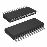
4KB 4K x 8 FLASH 8-Bit Microcontroller HC08 Series MC908JL3 28-SOIC (0.295, 7.50mm Width)
In Stock : Please Submit RFQ TO US
Need wholesale pricing? Send RFQ now for the best rates and immediate response.
QUICK RFQ
ADD TO RFQ LIST
Tech Specifications
Program Memory Type
FLASH
Surface Mount
YES
Terminal Position
DUAL
Package / Case
28-SOIC (0.295, 7.50mm Width)
JESD-30 Code
R-PDSO-G28
Data Converter
A/D 12x8b
Terminal Form
GULL WING
Number of Terminations
28
ROM (words)
4096
ECCN Code
EAR99
Qualification Status
Not Qualified
Voltage - Supply (Vcc/Vdd)
2.7V~3.3V
RoHS Status
ROHS3 Compliant
Moisture Sensitivity Level (MSL)
3 (168 Hours)
Supply Current-Max
11mA
Speed
8MHz
Operating Temperature
-40°C~85°C TA
HTS Code
8542.31.00.01
RAM Size
128 x 8
Number of I/O
23
Peripherals
LED, LVD, POR, PWM
Bit Size
8
Mounting Type
Surface Mount
Power Supplies
3/5V
Factory Lead Time
11 Weeks
Oscillator Type
External
Series
HC08
Core Size
8-Bit
Packaging
Tube
Part Status
Not For New Designs
Published
2004
Program Memory Size
4KB 4K x 8
Terminal Pitch
1.27mm
Base Part Number
MC908JL3
MC908JL3ECDWE Documents
Download datasheets and manufacturer documentation for MC908JL3ECDWE
Related Parts
EP4CE40F29C7
Intel
5SGSMD3H3F35I4G
Intel
EP1AGX60CF484I6N
Intel
5AGXBA7D6F35C6G
Intel
EP4SGX290KF43I3G
Intel
T20Q144I4
Efinix, Inc.
AFS600-PQG208I
Microsemi Corporation
5SGXEB6R3F43C2G
Intel
A1425A-PLG84I
Microsemi Corporation
CCGM1A1-BGA324
Cologne Chip
5SGXMB5R3F43C2G
Intel
5SGXEA7K1F40C2G
Intel
M2GL010T-VFG256I
Microchip Technology
EP3C55F780I7
Intel
EP2C5T144I8N
Intel
EP3SE260F1517I4LG
Intel
LAE5UM-25F-6BG381E
Lattice Semiconductor Corporation
1ST110EN3F43I3VGAS
Intel
Shopping Guide
Payment Methods
Payment Methods include Prepayment TT (bank transfer), Western Union, and PayPal. Customers are responsible for shipping costs, bank charges, customs duties and taxes.
Shipping Rate
Shipments are made once a day around 5pm, excluding Sundays. Once shipped, the estimated delivery time is usually 5-7 business days, depending on the courier you choose.
Delivery Methods
Provide DHL, FedEx, UPS, EMS, SF Express and Registered Airmail International Delivery Service
Follow Us
Please find more information about us from below social media and interact with us!
Contact With Us
TOOLS
payment
Transportation
Trademark
All Rights Reserved © 2025 AMPHEO PTY LTD