


Lattice Semiconductor
LFE2-50SE-6FN484C
FPGAs (Field Programmable Gate Array)
LFE2-50SE-6FN484C
2-LFE2-50SE-6FN484C

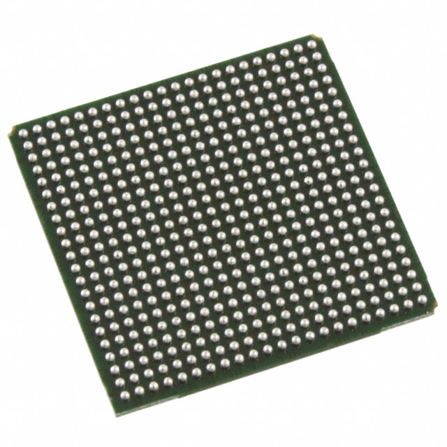
IC FPGA 339 I/O 484FBGA
In Stock : Please Submit RFQ TO US
Need wholesale pricing? Send RFQ now for the best rates and immediate response.
QUICK RFQ
ADD TO RFQ LIST
LFE2-50SE-6FN484C Description
ECP2 Field Programmable Gate Array (FPGA) IC 339 396288 48000 484-BBGA
Tech Specifications
Operating Temperature
0°C ~ 85°C (TJ)
Total RAM Bits
396288
Number of LABs/CLBs
6000
ECCN
3A991D
Number of I/O
339
Mounting Type
Surface Mount
Product Status
Active
Supplier Device Package
484-FPBGA (23x23)
Series
ECP2
Package / Case
484-BBGA
Voltage - Supply
1.14V ~ 1.26V
REACH Status
REACH Unaffected
Mfr
Lattice Semiconductor Corporation
HTSUS
8542.39.0001
Package
Tray
Number of Logic Elements/Cells
48000
RoHS Status
ROHS3 Compliant
Base Product Number
LFE2-50
Moisture Sensitivity Level (MSL)
3 (168 Hours)
LFE2-50SE-6FN484C Documents
Download datasheets and manufacturer documentation for LFE2-50SE-6FN484C
Related Parts
APA1000-CGS624B
Microchip Technology
EP2AGX45DF25C6N
Intel
EP4SE360F35I4G
Intel
A3P1000-FPQ208
Actel
1SG211HN2F43E1VG
Intel
EP3C16F484C7
Intel
EP3SL50F484C4LG
Intel
EP2AGX260FF35I5
Intel
5SGXEABN2F46C2G
Intel
XCV300-5FG456I
AMD
1ST210EU1F50E2LG
Intel
10AX090N1F45E1SG
Intel
LT1763CS8-1.8#TRPBF
Linear Technology
AX1000-BG729I
Microchip Technology
LFSC3GA80E-5FFN1704C
Lattice Semiconductor Corporation
A54SX32-2BG313I
Microsemi Corporation
XC2V1500-4BG575I
AMD
Shopping Guide
Payment Methods
Payment Methods include Prepayment TT (bank transfer), Western Union, and PayPal. Customers are responsible for shipping costs, bank charges, customs duties and taxes.
Shipping Rate
Shipments are made once a day around 5pm, excluding Sundays. Once shipped, the estimated delivery time is usually 5-7 business days, depending on the courier you choose.
Delivery Methods
Provide DHL, FedEx, UPS, EMS, SF Express and Registered Airmail International Delivery Service
Follow Us
Please find more information about us from below social media and interact with us!
Contact With Us
TOOLS
payment
Transportation
Trademark
All Rights Reserved © 2025 AMPHEO PTY LTD