


ON Semiconductor
LC898212XD-SH
FPGAs (Field Programmable Gate Array)
LC898212XD-SH
2-LC898212XD-SH
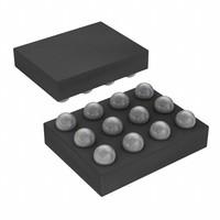
1.37mm mm Motor Drivers 12 1.77mm mm
In Stock : Please Submit RFQ TO US
Need wholesale pricing? Send RFQ now for the best rates and immediate response.
QUICK RFQ
ADD TO RFQ LIST
LC898212XD-SH Description
Tech Specifications
Mount
Surface Mount
Output Configuration
Half Bridge (2)
Terminal Finish
Tin/Silver/Copper (Sn/Ag/Cu)
Radiation Hardening
No
Function
Driver - Fully Integrated, Control and Power Stage
Height Seated (Max)
0.69mm
Terminal Position
BOTTOM
Package / Case
12-XFBGA, WLCSP
Logic Function
AND
Lifecycle Status
ACTIVE (Last Updated: 6 days ago)
Voltage - Supply
2.6V~3.6V
Terminal Form
BALL
Number of Pins
12
Number of Terminations
12
Width
1.37mm
Lead Free
Lead Free
Pbfree Code
yes
RoHS Status
ROHS3 Compliant
Moisture Sensitivity Level (MSL)
1 (Unlimited)
HTS Code
8542.39.00.01
Telecom IC Type
TELECOM CIRCUIT
Applications
Camera
Voltage - Load
2.6V~3.6V
Mounting Type
Surface Mount
JESD-609 Code
e1
Factory Lead Time
4 Weeks
Length
1.77mm
Contact Plating
Copper, Silver, Tin
Packaging
Tape & Reel (TR)
Part Status
Active
Published
2013
Terminal Pitch
0.4mm
Interface
I2C
LC898212XD-SH Documents
Download datasheets and manufacturer documentation for LC898212XD-SH
Related Parts
A1240A-1PG132C
Microsemi Corporation
10AX022E3F29I1HG
Intel
ICE40LP1K-QN84
Lattice Semiconductor Corporation
1SG211HN3F43E3XG
Intel
10AX032H4F35E3SG
Intel
5SGXEA7K1F40I2G
Intel
EP4CGX110DF31I7
Intel
EP4SGX290FH29I3
Intel
EP3CLS70F780I7
Intel
EP4SE820H35I4
Intel
EP2C20F484C8N
Intel
5SGSMD3H3F35I3L
Intel
EP2AGX190FF35I5N
Intel
5SGXMA4K3F40I3G
Intel
EP4SE360F35I3G
Intel
1SG250HH1F55I2VG
Intel
Shopping Guide
Payment Methods
Payment Methods include Prepayment TT (bank transfer), Western Union, and PayPal. Customers are responsible for shipping costs, bank charges, customs duties and taxes.
Shipping Rate
Shipments are made once a day around 5pm, excluding Sundays. Once shipped, the estimated delivery time is usually 5-7 business days, depending on the courier you choose.
Delivery Methods
Provide DHL, FedEx, UPS, EMS, SF Express and Registered Airmail International Delivery Service
Follow Us
Please find more information about us from below social media and interact with us!
Contact With Us
TOOLS
payment
Transportation
Trademark
All Rights Reserved © 2025 AMPHEO PTY LTD